


")


During Hot Chips 34, NVIDIA confirmed new details about its Grace CPU, Orin SOC, and NVLINK chip connectors.
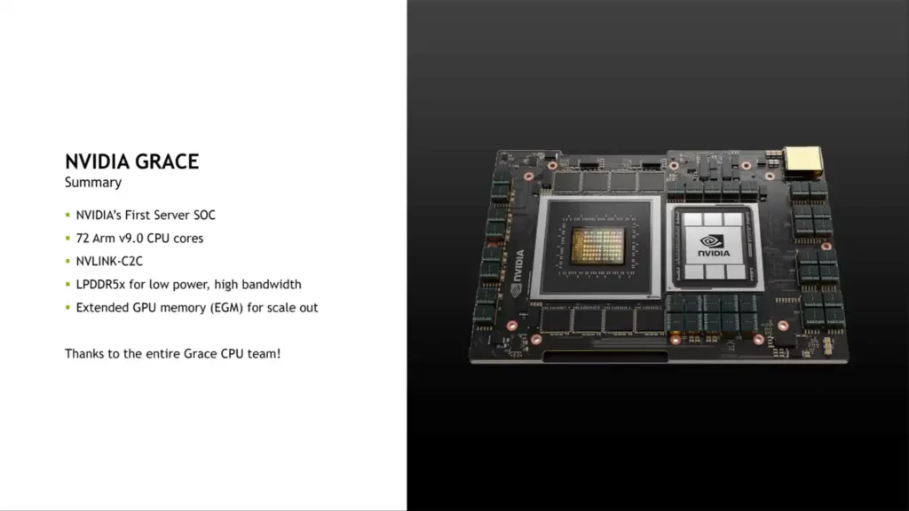
NVIDIA’s Grace CPU Breaks Cover features 72 Arm v9.0 Cores Per Chip, 117 MB L3 Cache, and 68 Gen 5 Lanes, All on TSMC 4N Process Node
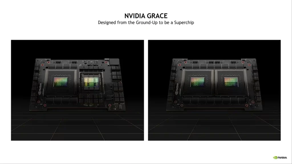
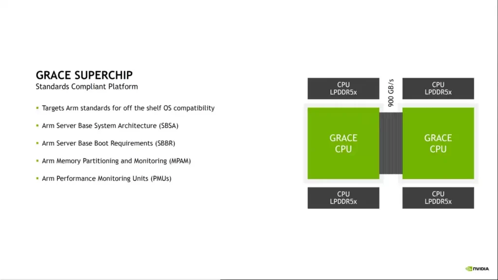
NVIDIA first revealed its Grace CPU and Superchip design at GTC 2022. The Grace CPU is NVIDIA’s 1st processor built on a custom Arm architecture, aimed at the server / HPC market. The CPU is available in two Superchip variants: a Grace Superchip module with two Grace CPUs and a Grace+Hopper Superchip control unit with one Grace CPU connected to a Hopper H100 GPU.
Grace’s main highlights are as follows-
- CPU with high performance for HPC and cloud computing
- Superchip architecture with up to 144 Arm v9 CPU cores
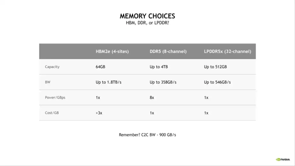
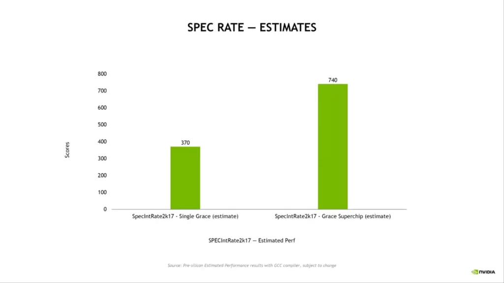
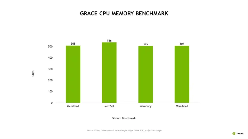
- The world’s first LPDDR5x memory with ECC, with a total bandwidth of 1TB/s SPECrate2017 int base over 740 (estimated)
- 7X faster than PCIe Gen 5 at 900 GB/s coherent interface
- DIMM-based solutions have twice the packaging density.
- 2X the performance per watt of today’s most powerful CPU
- All NVIDIA software stacks and platforms, including RTX, HPC, AI, and Omniverse, are supported.
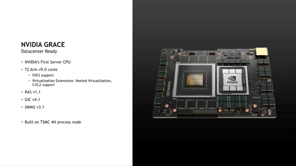
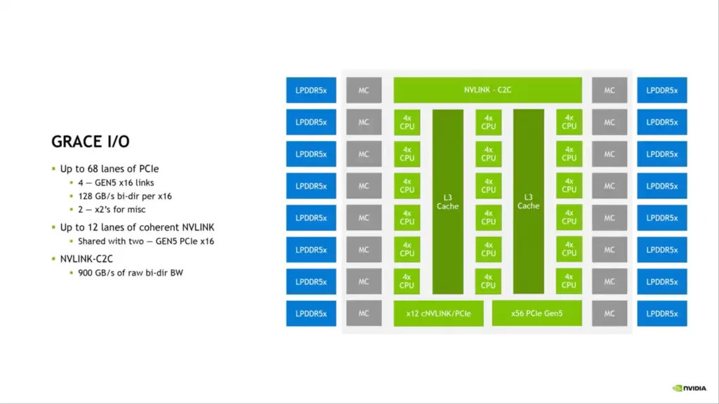
Grace, NVIDIA’s first server CPU, has 72 Arm v9.0 cores and supports SVE2 as well as characteristics associated additions such as Nested Virtualization and S-EL2. The CPU is built on TSMC’s 4N process node, an optimized edition of the 5nm process node explicitly designed for NVIDIA.
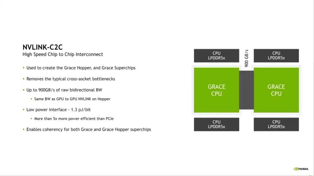
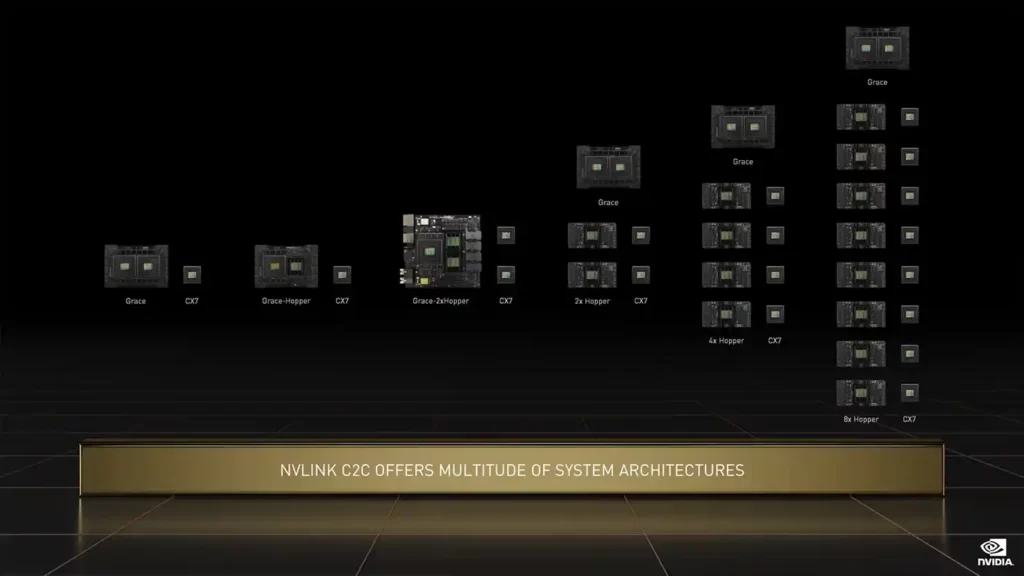
Grace is meant to be paired, so one of the most critical aspects of the design is the C2C (Chip-to-Chip) interconnect. Grace accomplishes this through NVLINK, which is used to manufacture the Superchips and eliminates all bottlenecks linked with a typical cross-socket structure.
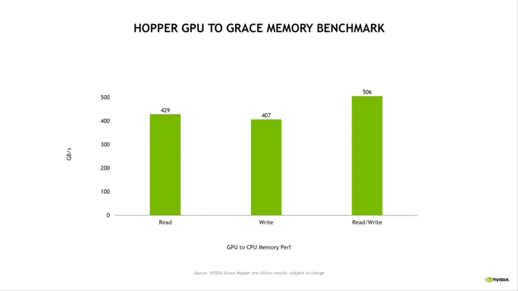
The C2C NVLINK connections give 900 GB/s of the raw bi-directional frequency band (the same as a GPU to GPU NVLINK switch on Hopper) while consuming only 1.3 PJ/bit of power, making it 5 times more effective than the PCIe framework.
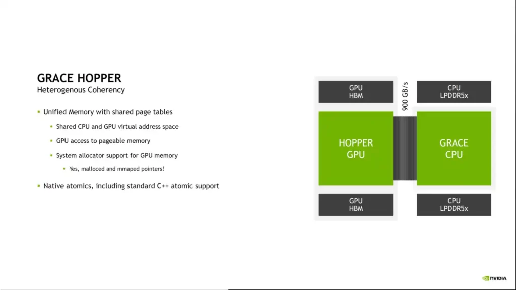
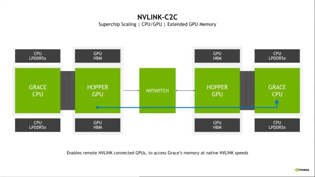
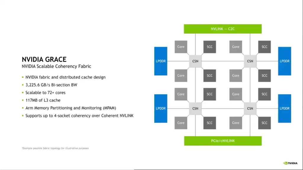
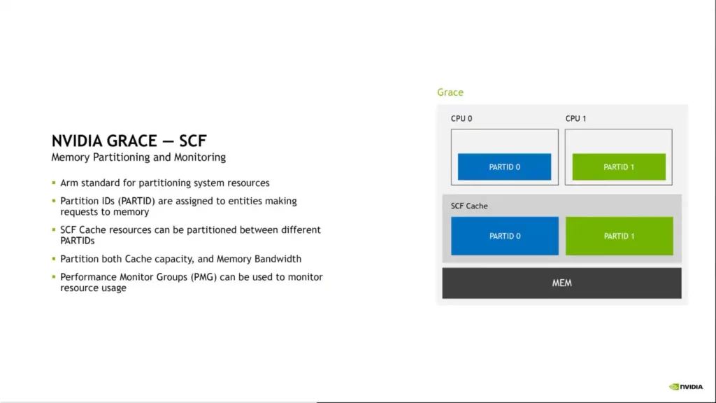
The NVIDIA Grace CPU has an optimized cohesion fabric and a shared cache design. The chip has a bi-section frequency band of up to 3.225 TB/s, is expandable beyond 72 cores (144 on Superchip), includes 117 MB of L3 cache, and supports Arm memory partitioning and monitoring (MPAM). Grace also enables cohesive memory architectures with shared page tables. A Grace CPU on one Superchip can interact directly with the GPU on the other chip and even connect directly to its VRAM at native NVLINK speeds when two NVIDIA Grace+Hopper Superchips are linked via an NVSwitch.
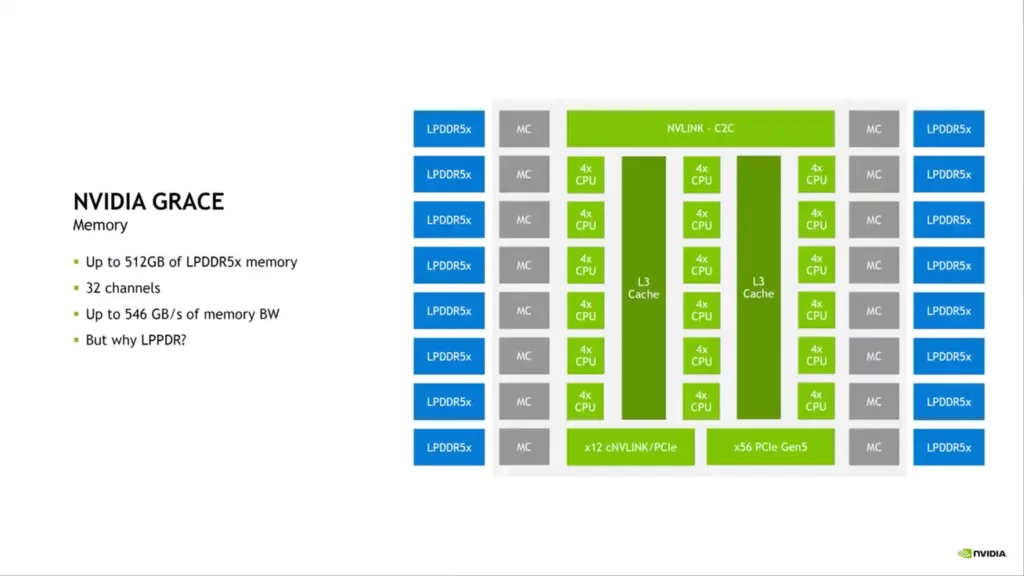

Regarding memory configuration, NVIDIA uses up to 512 GB of LPDDR5X across 32 channels, supplying up to 546 GB/s of memory bandwidth. According to NVIDIA, LPDDR5X offers the best value when considering the overall frequency band, cost, and power consumption. There are 68 PCIe Gen 5.0 lanes for I/O, four of which can be used for x16 links at 128 GB/s and the other two for MISC. 12 NVLINK lanes are shared by two Gen 5 PCIe x16 links.
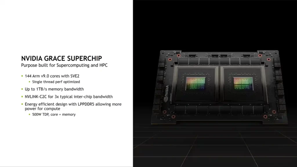
Regarding TDP, the NVIDIA Grace (CPU Only) Superchip is optimized for single-core performance, with a memory bandwidth of up to 1 TB/s and a TDP of 500W for the 144-core dual chip configuration.
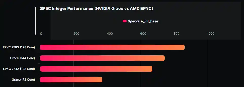
This isn’t a significant difference in performance, but we’d prefer to see the performance indicators. The Grace SUPERCHIPS are scored at around 500W. In contrast, each AMD EPYC 7763 chip has a TDP of 280W, so two of them will be around 560W if we don’t factor in the additional system power requirements, whereas NVIDIA’s 500W figure is for the entire GRACE SUPERCHIP package.
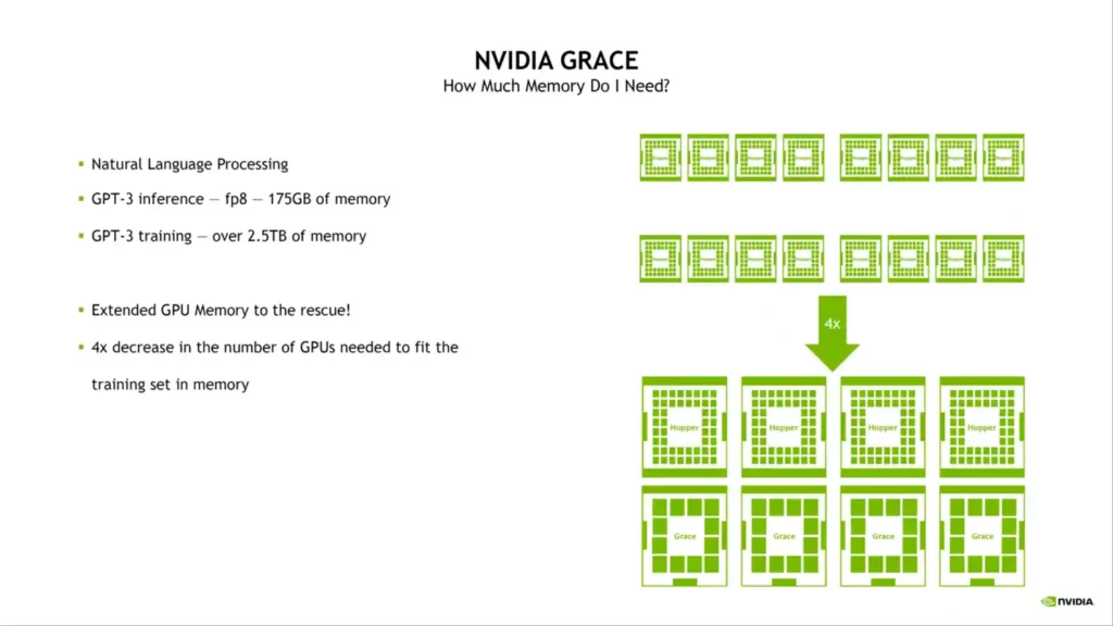
According to NVIDIA, Grace is a highly specialized processor aimed at workflows such as having trained next-generation NLP models with over 1 trillion variables. A Grace CPU-based system, when closely linked with NVIDIA GPUs, will deliver 10x faster performance than today’s state-of-the-art NVIDIA DGX-based systems, which run on x86 CPUs.
It will be exciting to observe how the Grace CPUs compare to x86 chips, but by the time they are available, they will compete with AMD’s Genoa and Intel’s Sapphire Rapids CPUs. As previously reported, the NVIDIA Grace CPUs will be utilized in the ATOS supercomputer.


