

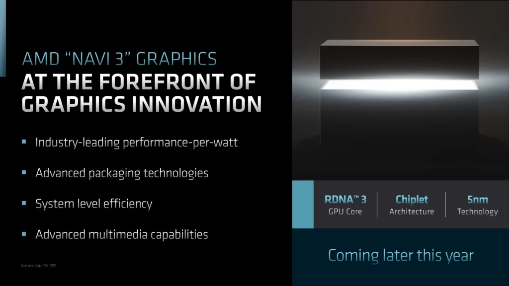
The Navi 31, AMD’s reported flagship GPU for the forthcoming RDNA 3 generation and a product of TSMC’s 5nm production node, has been given die size.
AMD RDNA 3 “Navi 31” GPU Die size leaked online which Reportedly Measures Around 350mm2 and 33% Smaller on TSMC’s 5nm Node
Greymon55, who released the claimed die size of the next-generation GPU powerhouse from camp red, is the source of the claims. The following are some of the significant RDNA 3 GPU characteristics that AMD will focus on:
- 5nm Process Node
- Advanced Chiplet Packaging
- Rearchitected Compute Unit
- Optimized Graphics Pipeline
- Next-Gen AMD Infinity Cache
- >50% Perf/Watt vs RDNA 2
The AMD RDNA 3 GPU was rumored to have a total die area of 600 mm2, but the real GPU die size would be nearly half that. The entire die package will include both the cache “MCDs” and the GPU “GCD,” which is why. According to the earlier report, the highest Navi 31 GPU will
have six RDNA 3 MCDs. Although they will be fused into one package, each MCD will differ from the GCD. The RDNA 3 Navi 31 GCD will have a smaller die size, roughly 350mm2.

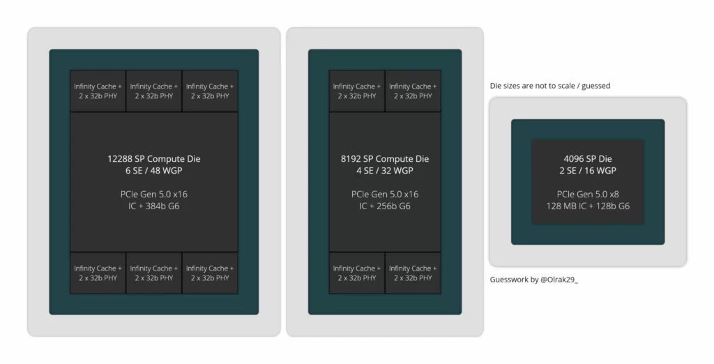
Compared to AMD’s current Navi 21 RDNA 2 GPU, which has a die size of 520mm2, the TSMC 5nm production node results in a 33% size reduction. On the other hand, the MCDs are anticipated to be produced on TSMC’s 6nm process node. The staff at 3DCenter have done an
intriguing comparison, stating that the Navi 21 GPU will have a die size of about 375mm2 without the Infinity Cache & memory controllers. That makes it comparable to the Navi 31 GPU, but the new flagship has more than twice as many cores. If the new chip were to be built on the older 7nm node, the GPU die might be more significant than 500 mm2.

Additionally, @Kepler L2 notes that to save space, the RDNA 3 GPU architecture used in the Navi 31 SKU has eliminated many on-die technologies like XGMI, GDS (Global Data Share), the Legacy Geometry Pipeline, and Legacy Scan Converter. Since the RDNA 3 GPUs do not
have specific GPU capabilities, they are likely unnecessary.
Additionally, @Kepler L2 notes that to save space, the RDNA 3 GPU architecture used in the Navi 31 SKU has eliminated many on-die technologies like XGMI, GDS (Global Data Share), the Legacy Geometry Pipeline, and Legacy Scan Converter. But since RDNA 3 GPUs do not
have specific GPU capabilities, they are likely unnecessary.
AMD Radeon RX 7900 XT Graphics Card Specifications
The Radeon RX 7900 XT graphics card and other next-generation enthusiast cards would be powered by AMD Navi 31 GPU, the top-tier RDNA 3 processor. We’ve heard that AMD would replace its next-generation RDNA 3 GPUs’ compute units with workgroup processors.
Dual CU (Compute Units) will be housed in each WGP, but there will be four SIMD32 clusters per CU instead of two on each CU in RDNA 2. According to rumors, AMD has the choice of the 6nm die from TSMC or Samsung.
According to the most recent information, the AMD Navi 31 GPU with RDNA 3 architecture is anticipated to feature a single GCD with 48 WGPs, 12 SAs, and 6 SEs. This will distribute 12,288 stream processors, fewer than the previous tally. The Navi 31 GPU will also include 6
MCDs, each of which will have a 64 MB Infinity Cache and maybe also the 64-bit (32-bit x 2) memory controllers, giving the device a 384-bit bus interface. This will also reduce total computing performance until AMD overclocks its flagship part to over 3.0 GHz.

Even though AMD has continuously outperformed NVIDIA in terms of clock speeds over the previous generation, this trend is predicted to continue. The AMD Navi 31 GPU is rumored to have clock rates that can reach or even exceed 3 GHz. The top-tier GPUs from NVIDIA also
have clock rates that are nearly 2.8 GHz. With a 3 GHz clock speed, the most recent flagship can execute over 75 TFLOPs of FP32 processes, which is a 2.3x increase over the RX 6950 XT, the RDNA 2 flagship.
As a result, there will be a higher power draw, and AMD appears to have confirmed this. However, their array of next-generation graphics cards will still be more energy-efficient than what NVIDIA has to offer, despite having higher power usage. For a >2x performance increase,
the Radeon RX 7900 XT’s TBP should wind up being close to 400–450W, given that the AMD Radeon RX 6950 XT already has a TBP of 335W.
When it is released later this year, the AMD Navi 31 GPU will face off against the claimed 600W and 600mm2 NVIDIA AD102 GPU that makes use of the Ada Lovelace graphics architecture.
News source: wccftech.com
Check out more:
- Top 5 best wireless gaming keyboards in 2022
- Top 5 gaming laptops in 2022
- Top 5 PC Cabinets in 2022
- Top 5 PCIe 4.0 SSD for gaming in 2022
- Top 5 AMD Motherboards in 2022
- Best 5 gaming headsets in 2022
- Top 5 Gaming CPUs in 2022: First Quarter of 2022
- Top 5 Best gaming monitors in 2022
- Top 5 best power supplies for gaming in 2022
- Top 5 Best Graphics Cards for Gaming in 2022
- Top 5 best gaming PC in 2022
- Top 5 Best Intel B660 Motherboards in 2022
- Top 5 Best lightweight gaming mouse in 2022
- The top 5 best FreeSync monitors in 2022
- Top 5 Best Budget B660 Motherboards (DDR4 Variant)
- Top 5 Best AMD B550 Motherboards in 2022
- Top 5 Best cheap microphones for gaming and streaming


