

NVIDIA has published a detailed analysis of their next-generation Grace CPU Superchip, which would outperform AMD EPYC CPUs by up to 2.5 times.
NVIDIA Shows Up To 2.5x Performance & 3.5x Efficiency Gain With Grace CPU Superchip Versus AMD EPYC Milan-
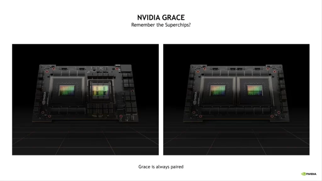
At GTC 2022, NVIDIA debuted its Grace CPU and related Superchip architecture. The Grace CPU is NVIDIA’s first processor built on a unique Arm architecture and is targeted at the server and high-performance computing markets. Two Superchip variants of the CPU are available: a Grace Superchip module with two Grace CPUs and a Grace+Hopper Superchip with a single Grace CPU coupled to a Hopper H100 GPU.


The following are some of Grace’s key highlights:
- High-performance CPU for HPC and cloud computing
- Super chip design with up to 144 Arm v9 CPU cores
- World’s first LPDDR5x with ECC Memory, 1TB/s total bandwidth
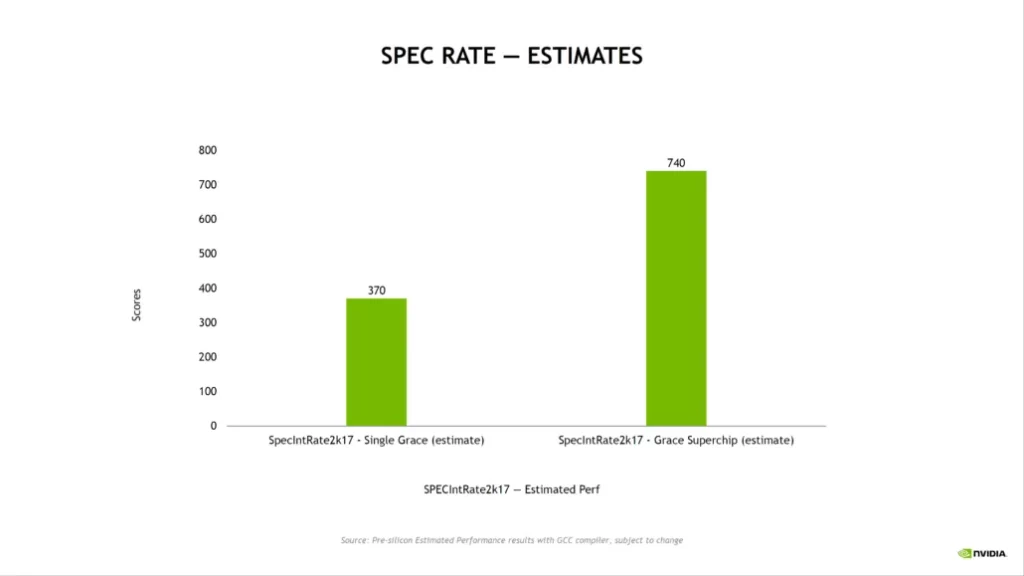
- SPECrate2017_int_base over 740 (estimated)
- 900 GB/s coherent interface, 7X faster than PCIe Gen 5
- 2X the packaging density of DIMM-based solutions
- 2X the performance per watt of today’s leading CPU
- Runs all NVIDIA software stacks and platforms, including RTX, HPC, AI, and Omniverse
NVIDIA Grace CPU Superchip architecture features
| Core architecture | Neoverse V2 Cores: Armv9 with 4x128b SVE2 |
| Core count | 144 |
| Cache | L1: 64 KB I-cache + 64 KB D-cache per core L2: 1 MB per core L3: 234 MB per superchip |
| Memory technology | LPDDR5X with ECC, co-packaged |
| Raw memory BW | Up to 1 TB/s |
| Memory size | Up to 960 GB |
| FP64 peak | 7.1 TFLOPS |
| PCI Express | 8x PCIe Gen 5 x16 interfaces; option to bifurcate Total 1 TB/s PCIe bandwidth. Additional low-speed PCIe connectivity for management. |
| Power | 500 W TDP with memory, 12 V supply |
Grace, NVIDIA’s first server CPU, has 72 Arm v9.0 cores and supports Nested Virtualization, S-EL2, SVE2, and other cloud computing extensions. The 4N process node from TSMC, an improved 5nm manufacturing node designed specifically for NVIDIA, is used to manufacture the CPU. Peak FP64 performance on the new architecture can reach up to 7.1 TFLOPs.

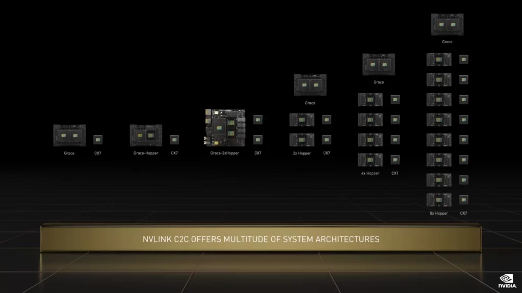
Grace’s C2C (Chip-To-Chip) interface represents one of the most important features of the design because it is intended to be used in pairs. Grace does this by eliminating all bottlenecks connected to a traditional cross-socket arrangement using NVLINK, which is employed to create the Superchips.
The C2C NVLINK connection operates with an extremely low wattage interface of just 1.3 pJ/bit or 5 times more efficient than the PCIe protocol, and it offers 900 GB/s of raw bi-directional capacity the same connectivity as a GPU to GPU NVLINK switch on Hopper.

nvidia grace cpu superchips hot chips 34 image slide 1 
nvidia grace cpu superchips hot chips 34 image slide 2 
nvidia grace cpu superchips hot chips 34 image slide 3 
nvidia grace cpu superchips hot chips 34 image slide 4 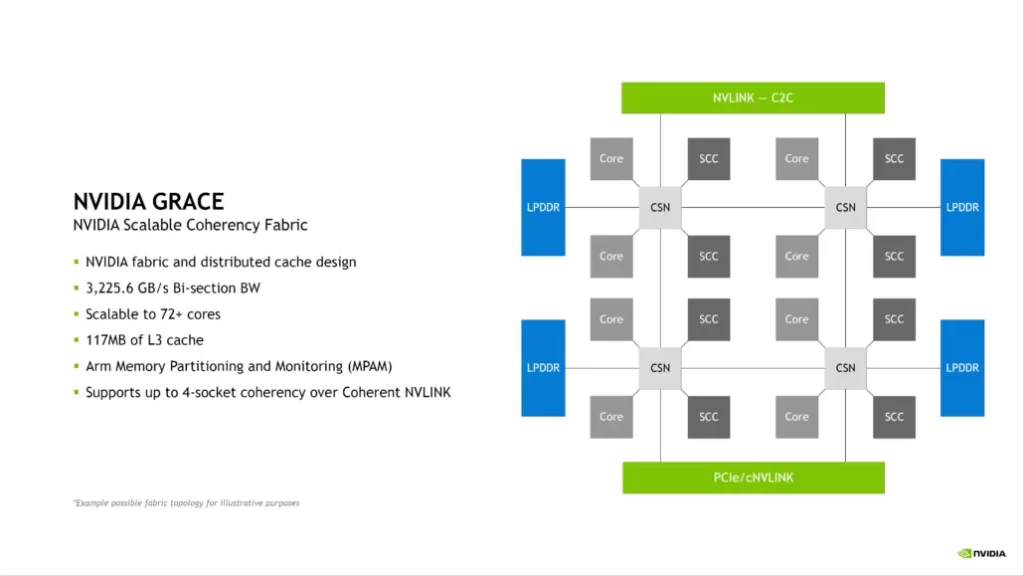
nvidia grace cpu superchips hot chips 34 image slide 5 
nvidia grace cpu superchips hot chips 34 image slide 6
A dispersed cache and extensible cohesion fabric are two aspects of the NVIDIA Grace CPU. The device includes 117 MB of L3 cache per core or 234 MB per Superchip, has up to 3.225 TB/s of bi-section bandwidth, is scaleable beyond 72 cores 144 on Superchip, and supports Arm memory segmentation and monitoring (MPAM). Grace also permits shareable page tables for a unified memory architecture. A Grace CPU on one Superchip can interact directly with the GPU on the other Superchip and even utilize its VRAM at native NVLINK speeds when two NVIDIA Grace+Hopper Superchips are coupled by an NVSwitch.
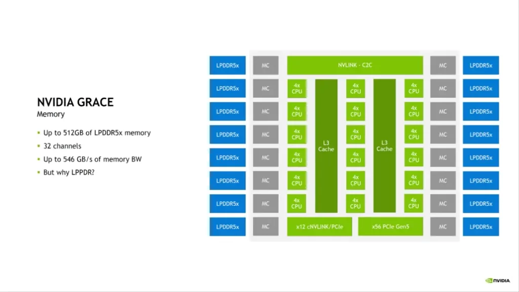
In order to achieve up to 1 TB/s of memory bandwidth, NVIDIA is using up to 960 GB of LPDDR5X (ECC) across 32 channels in the memory architecture of Grace. According to NVIDIA, when considering the entire bandwidth, cost, and power demand, LPDDR5X offers the best value. For instance, compared to DDR5, the LPDDR5X subsystem offers 53% higher bandwidth at 1/80th the power consumption per GB/s and at a comparable price. More bandwidth and efficiency may have been achieved with HBM2e memory, but at a 3x price premium.
68 PCIe Gen 5.0 lanes are available for I/O, four of which can be used for x16 links at 128 GB/s, and the remaining two are reserved for MISC. Additionally, two Gen 5 PCIe x16 links share 12 coherent NVLINK lanes.


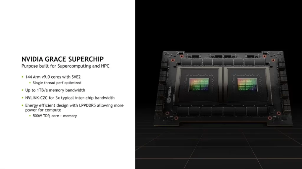
The NVIDIA Grace (CPU Only) Superchip has a TDP of 500W for the 144-core dual chip configuration, 1 TB/s of memory bandwidth, and is single-core performance oriented.
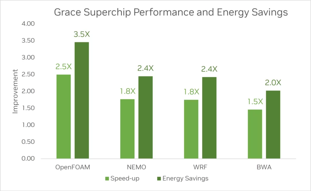
NVIDIA’s performance statistics pit the Grace CPU Superchip against dual-socket AMD EPYC 7763 “Milan” CPUs on a variety of HPC workloads, including OpenFOAM, WRF, NEMO, and BWA. The Grace CPU Superchip offers a remarkable 2.5x speed gain in OpenFOAM with up to 3.5x efficiency. In comparison to AMD’s EPYC Milan CPUs, NVIDIA’s new Grace CPU Superchip should be able to give an average performance boost of 1.9x and a watt-performance boost of 2.57x. Additionally, this ought to produce performance that is comparable to that of the most recent AMD and Intel server CPUs.
NVIDIA Grace CPU Superchip vs AMD EPYC 7763 Milan CPUs


According to NVIDIA, the Grace processor is highly specialized and is intended for workloads like developing next-generation NLP models with more than a trillion parameters. A Grace CPU-based system will run 10 times quicker than the most advanced NVIDIA DGX-based systems available today when firmly paired with NVIDIA GPUs.
When the Grace CPUs are released, they will be up against AMD’s Genoa and Intel’s Sapphire Rapids CPUs, therefore it will be exciting to observe how they compare to x86 processors. According to this rumor, the ATOS supercomputer will employ NVIDIA Grace CPUs.
Source: wccftech.com


